Mastering of nano- and microstructures
Before a nano- or microstructure can be used in a product with a functional surface, the structures must be produced in a mastering process. For this, we have laser interference lithography and UV lithography.

Laser interference lithography (LIL)
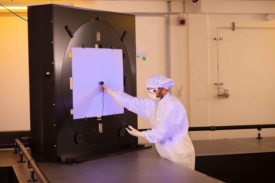
Laser interference lithography is a maskless lithography technique for creating periodic grating structures using two interfering laser beams.
We use laser interference lithography and UV lithography to realize a variety of nano- and microstructures. These technologies can be used to master structures with periods ranging from 200 nanometers to several hundred micrometers.
We pay particular attention to large-area, seamless end products with total areas of up to one square meter. The strength of laser interference lithography is the ability to upscale to very large patterned areas with excellent homogeneity. The technology enables the mastering of periodic or stochastic structures seamlessly on an area of up to 1m².
UV Lithography
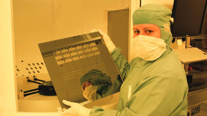
temicon uses UV lithography as a mastering process for microstructures of more than 1 µm structure size. Through UV lithography, microstructures of any geometry can be processed on an area of up to 20" x 24".
Special features of temicon technology are e.g. large formats in the square meter range, high aspect ratio of more than 2.0, sidewall angles of 85° ± 2°, which allow demolding of the structure in the production process or gapless microlens arrays.
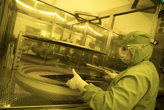
Due to these innovations, we realize a particularly wide range of microstructures with customized functions for our customers. A production line for UV photolithography for wafer sizes up to 200 mm is installed in our 400 m² clean room. This also includes resist coating, exposure, wet processes and sputtering.
20"x 24"
1m²
200nm


Consultation
We will be happy to advise you.
Which nano- or microstructures would you like for your products? Call us! Benefit from our expertise

