Microstructures in Optics
A world without micro- and nanostructured optical components can hardly be imagined anymore. We deliver key components for 3D sensors, optical measurement technology and industrial automation to series customers worldwide.
Micro- and nanooptics make our customers’ optical systems more efficient, powerful and precise. Whether structured light, antireflection or solid angle filters, the applications for microoptical systems are very broad.

Katrin Christiani
Product Manager Optics


Wafer Level Optics
Microlens arrays in large quantities
Replication by the UV imprint process process at wafer level allows cost-efficient production of large quantities. Above all, microlens arrays (MLA) with spherical or aspherical lens geometries are used for 3D sensors to provide automated face or component recognition according to the structured light principle.
45.000
100%
10nm

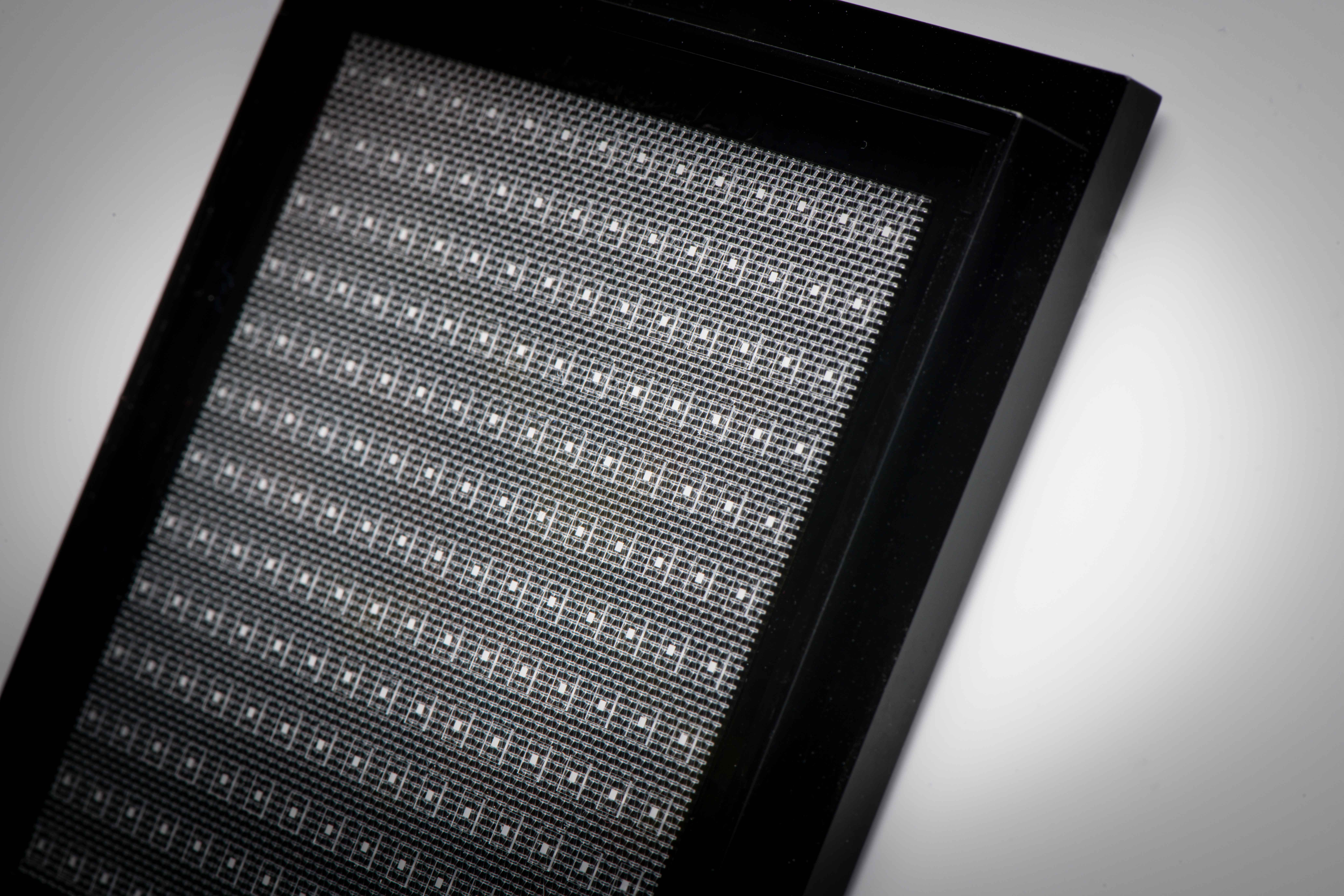

ANGLE-SELECTIVE ELEMENTS
Angle partitioning for defined solid angles
The combination of lens and pinhole has long been proven in optics. temicon has transferred this principle into micro-optics and can manufacture films less than 400 µm thick that create an angle partition.
Every microlens is assigned to a pinhole that is in the lens’s focal point. The high finish quality and extremely low tolerances in aligning pinholes allow efficient filtering of defined solid angles. This film is used in industrial measurement technology, among other applications.
0,4mm
90%
50µm

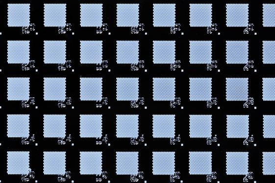

MOTH EYE STRUCTURES
Broadband antireflection over a wide angle with only one layer
Many optical applications require low reflection together with higher transmission.
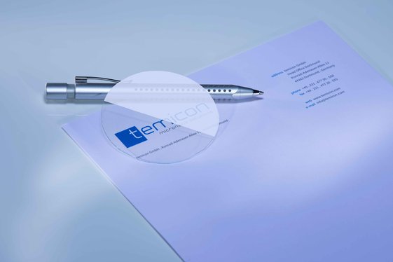
Copied from nature, temicons own antireflection structure is based on the moth eye principle and offers many advantages over thin-film antireflection coatings. It works across the entire visible spectrum. It has a high acceptance angle. Only one layer application is needed. It increases the transmission of glass in air from slightly above 92% to approx.99.5%. Applications include display technology and sensors.
0,2%
0,5%
1
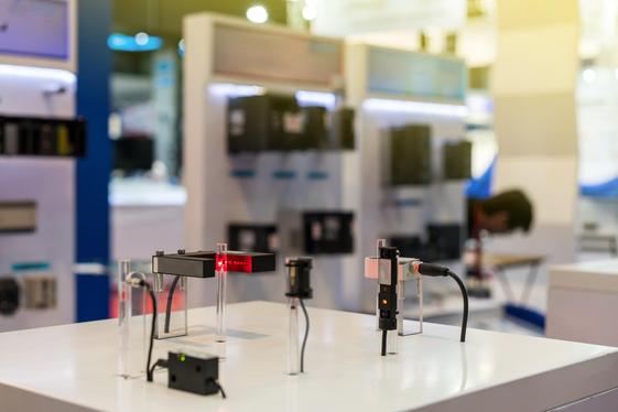

OPTICAL GRIDS
Linear and cross grids from sub-micron to 1m² surfaces
From several tens of microns to 200 nm, temicon offers a wide variety of optical grids.
Whether linear grids, cross grids or hexagonal grids, the orientation and arrangement is variable. Interference lithographic manufacturing of the grids allows grids up to about 1 m² to be exposed in one shot. With R2R processes, this grid's extremely large surfaces can be replicated. They are used in LED/OLED displays, in optical data transfer, optical measurement technology and in the packaging industry.
1m²
200nm
20m/min


PRECISION OPTICAL PARTS
Burr-free, high-precision components, such as slit and perforated sheets
Where metal etching ends, electroforming starts. Galvanic processing allows the greatest possible exactness in producing precision metal parts.
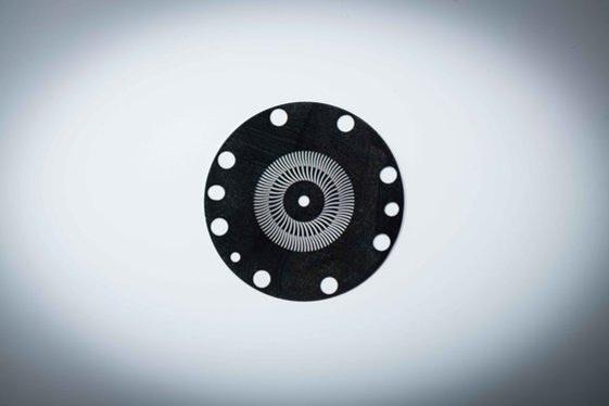
Burr-free manufacturing of the parts, combined with the unmatched small component tolerances adds considerable value to your product. Whether a slit plate, a perforated plate or an encoder disk, with the LIGA process, temicon offers products for all of these applications.
2µm
500nm
100%

Consultation
We will be happy to advise you.
Which nano- or microstructures would you like for your products? Call us! Benefit from our expertise
